
ASSEMBLY & SELECTION GUIDE
PCB Battery Connector Footprints: Separate Pads, Locating Holes and Reference Views
Use Kangsheng BC75 and BC82 recommended PCB layouts to separate pads, locating holes, outline dimensions and top-view references.
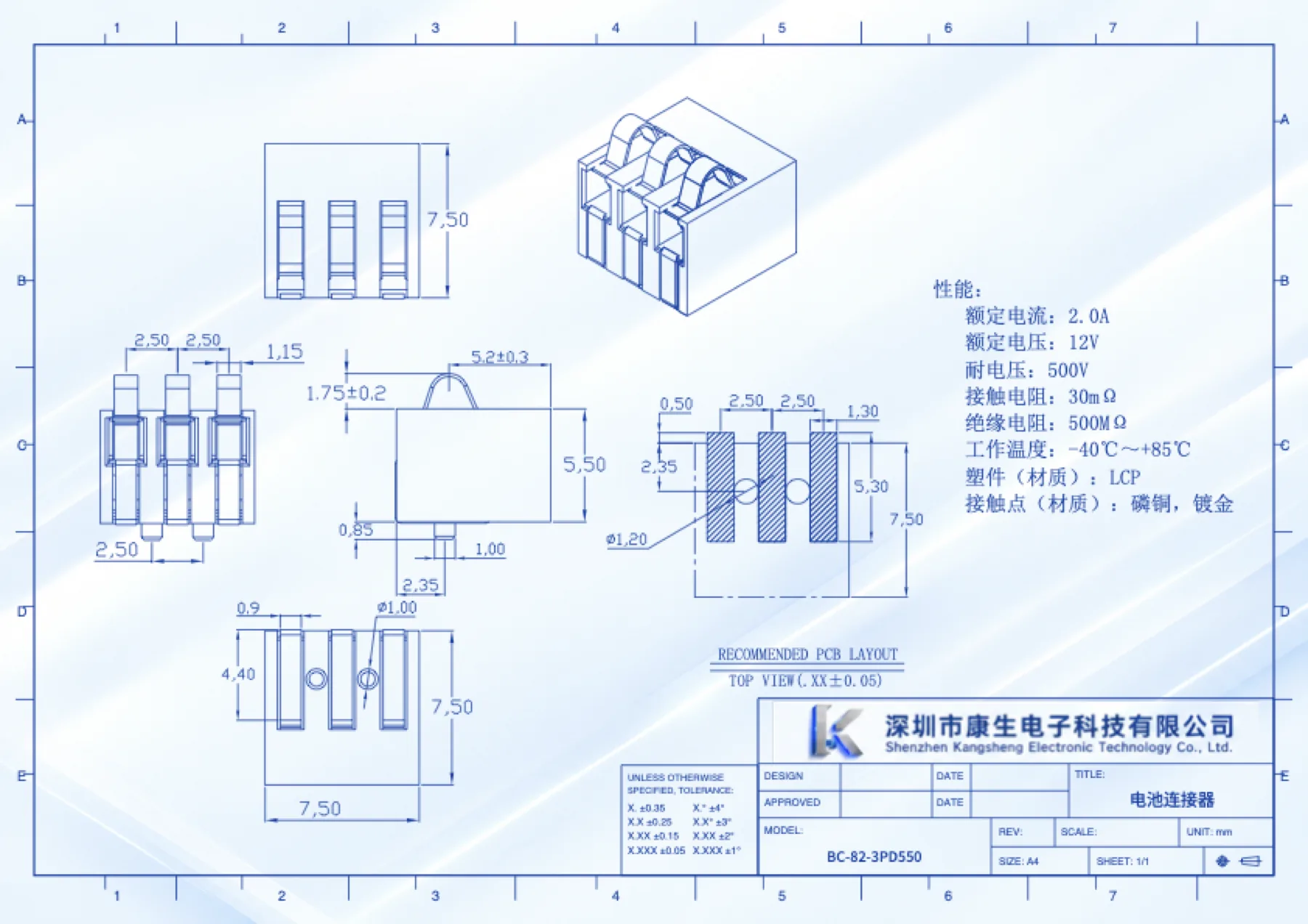
A PCB battery connector footprint needs the model's recommended board pattern, its view direction and its locating features. The connector's outside dimensions describe the component envelope; they are not a substitute for solder pads or hole locations. Read those features as separate sets of dimensions before entering them in a PCB library.
The Kangsheng BC-82-3PD550 and BC-75-3PD series drawings both include a region explicitly labelled RECOMMENDED PCB LAYOUT and TOP VIEW. They therefore provide a concrete place to begin. This article shows how to read that information and organise a board review without turning a different view or an unlabelled dimension into a pad recommendation.
After placing the footprint, check the assembled contact plane and compression stack.
Select the model and preserve the whole drawing
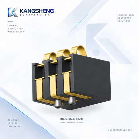
Start with the complete part number. BC-82-3PD550 is the three-pin, 2.5 mm pitch version listed with a 5.5 mm housing height. BC-82-4PD300 has four pins at the same listed pitch and a 3 mm housing height. A footprint entry named only “BC82” loses a difference that is visible before any dimensions are copied.
The BC-82 guide links both variants and their respective documents. Keep the model label, units, tolerance notes and recommended-layout region with the file. A cropped image of the terminals cannot provide all of that context.
Figure 1. BC-82-3PD550 original drawing. The outside views and the recommended board pattern appear on the same sheet, but their dimensions describe different features. Open the original BC-82-3PD550 PDF.
For BC-75, the 540 and 650 product records currently associate the same series PDF. Its part-number table gives A/B/C values for several versions. Select the appropriate row before reading the side and section views. Keep the model-specific STEP file alongside that series PDF; a common two-dimensional sheet does not make the CAD files interchangeable.
Keep the top-view convention explicit
A top view of the recommended PCB layout establishes a viewing convention for the pattern. A connector underside view elsewhere on the sheet is another view of the component. Copying an underside picture into a board pattern without checking orientation can put features on the wrong side of the intended reference.
Choose a reference feature and mark it consistently in the PCB library, the component drawing and the assembly view. Keep the board side and viewing direction in the review notes. If the project assigns contact numbers, add its pinout definition separately; three visible contacts do not identify power, return or signal functions.
Do not assign an electrical function to a locating hole. Its location can help align the component mechanically, but its purpose is different from the contact pads. Similarly, a housing edge used as an assembly reference is not automatically the footprint's electrical origin.
Read locating holes separately from soldering features
The BC-82-3PD550 component view calls out a Ø1.00 mm locating post; its recommended PCB layout calls out a Ø1.20 mm hole. Those are different features, so record both values rather than copying the post diameter into the board pattern. The PCB region is marked TOP VIEW (.XX ±0.05). Keep that local note with the PCB-layout dimensions; the component views retain their own dimension callouts.
The BC-75 recommended-layout region also separates the contact pattern from the larger support feature and locating holes. The contact pattern shows 2.50 spacing between adjacent contact positions. The product record's 2.5 mm pitch agrees with that spacing, but pitch alone does not define the whole footprint.
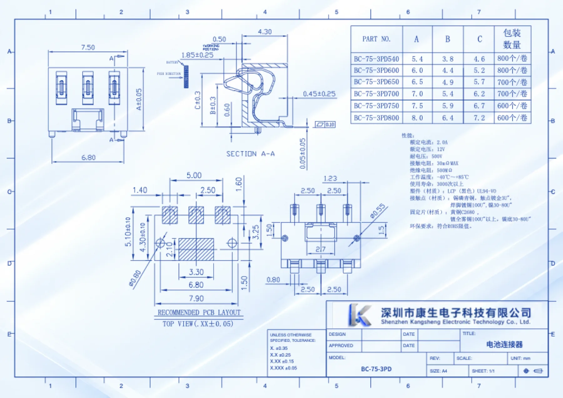
Figure 2. BC-75 series sheet. Read contact spacing, locating holes and the support feature individually. The section view and A/B/C model table serve the assembly review. Open the original BC-75 series PDF.
A useful reading sheet has separate entries for contact pitch, pad geometry, locating-hole geometry, support features and component outline. Record the drawing view beside each entry. This stops a clear-looking outside dimension from being carried into the pad table just because it was easy to find.
Do not create missing manufacturing layers from the outline
A recommended PCB pattern is a starting document, not evidence that every board-manufacturing layer has been specified. If the supplied sheet does not define solder-mask openings, stencil apertures or assembly courtyard requirements, do not label dimensions invented from the housing outline as the manufacturer's recommendations.
Keep those decisions with the board and assembly process review. Make the requested layer and feature explicit when asking the supplier for more information. “Please confirm the board pattern for this model” is useful; a marked request for the pad, locating-hole or stencil detail is more precise.
A STEP model helps examine component clearance and locating-feature positions in an assembly. Its existence does not establish a stencil design or a completed soldering process evaluation. Use the relevant BC-75 model and document links to keep the height variant associated with its CAD file.
Check model changes before reusing a PCB library entry
The two BC-82 examples have different pin counts and housing geometry. Treat a change from 3PD550 to 4PD300 as a new footprint and assembly review; a common pitch is not a complete substitution check.
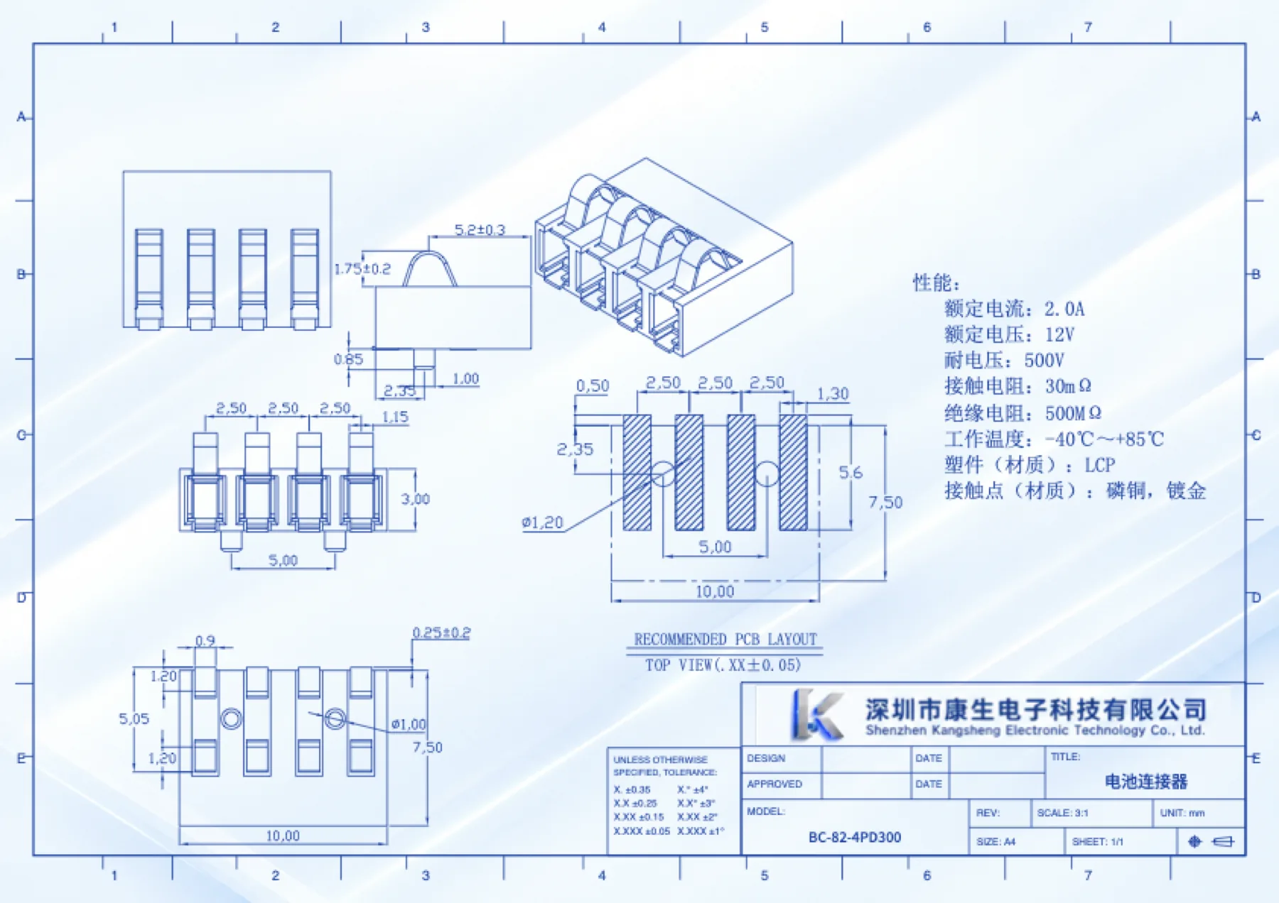
Figure 3. BC-82-4PD300 drawing. Compare its complete pattern and model identity with the three-contact file instead of adding a fourth pad to a remembered outline. Open the original BC-82-4PD300 PDF.
For BC-75-3PD540 versus BC-75-3PD650, the same series file is associated with both records and the A values are 5.4 and 6.5. That is evidence of a documented height distinction. It is not proof that every assembly condition, working contact position or process decision can be reused without review.
The linked drawings' REV fields are blank. Keep the original filename and the date on which the file was obtained. Before releasing a board design, request the currently applicable file and record that reply. Do not turn a download date into a fabricated design revision.
Send a marked board review rather than a bare part name
For the contact-loading direction, use the top-press vs side-press drawing guide. A board top view and the battery's insertion path answer different assembly questions.
Attach the exact connector model, original drawing file, selected series row where applicable, and a board image showing the intended top view. Mark the feature that needs an answer and keep the contact pinout with the project interface definition. Include the corresponding STEP filename if clearance is part of the question.
The BC-82-3PD550 product page provides that model's PDF and CAD files. For a side-press comparison, use the BC-75-3PD650 documents, then identify the 650 row in the series sheet.
Browse the spring battery connector category for other geometries. When a candidate is selected, submit the model, drawing and marked board references for an enquiry. Those references make the unresolved feature visible to both the PCB designer and the supplier.
Source: Kangsheng Electronics product records and original BC75/BC82 drawings.
CATALOGUE REFERENCES
Related products


YOUR NEXT DESIGN CHECK
Send us your drawing.
We’ll check pitch, height and compression against your assembly requirements.
Ask about this article