
ASSEMBLY & SELECTION GUIDE
2.5 mm Blade Connectors: PCB Footprint and Mounting Checks
Use four-position Kangsheng B01M and B04F drawings to review SMT and right-angle through-hole mounting before releasing a PCB footprint.
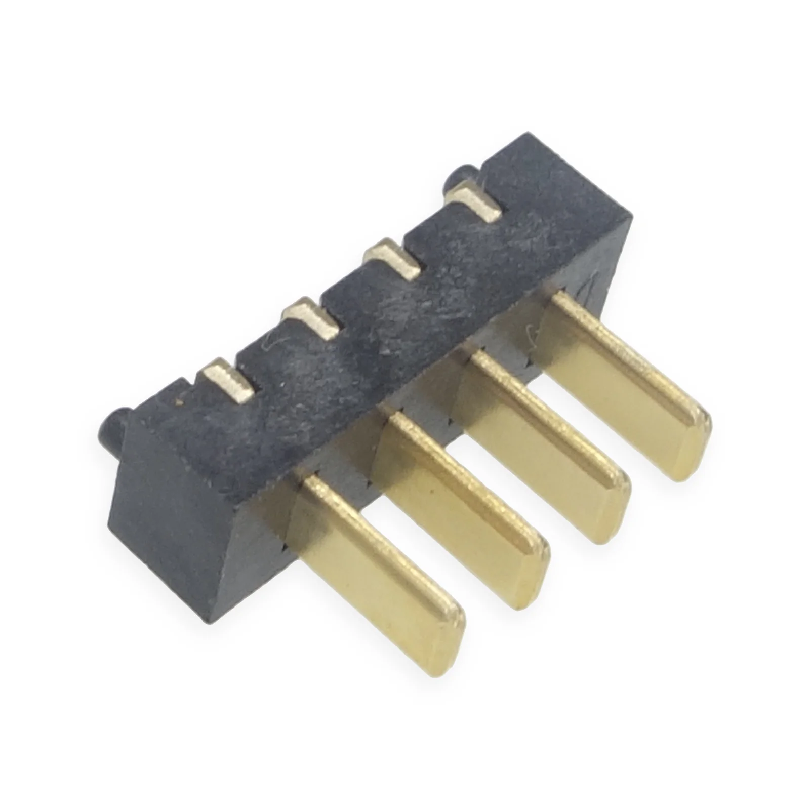
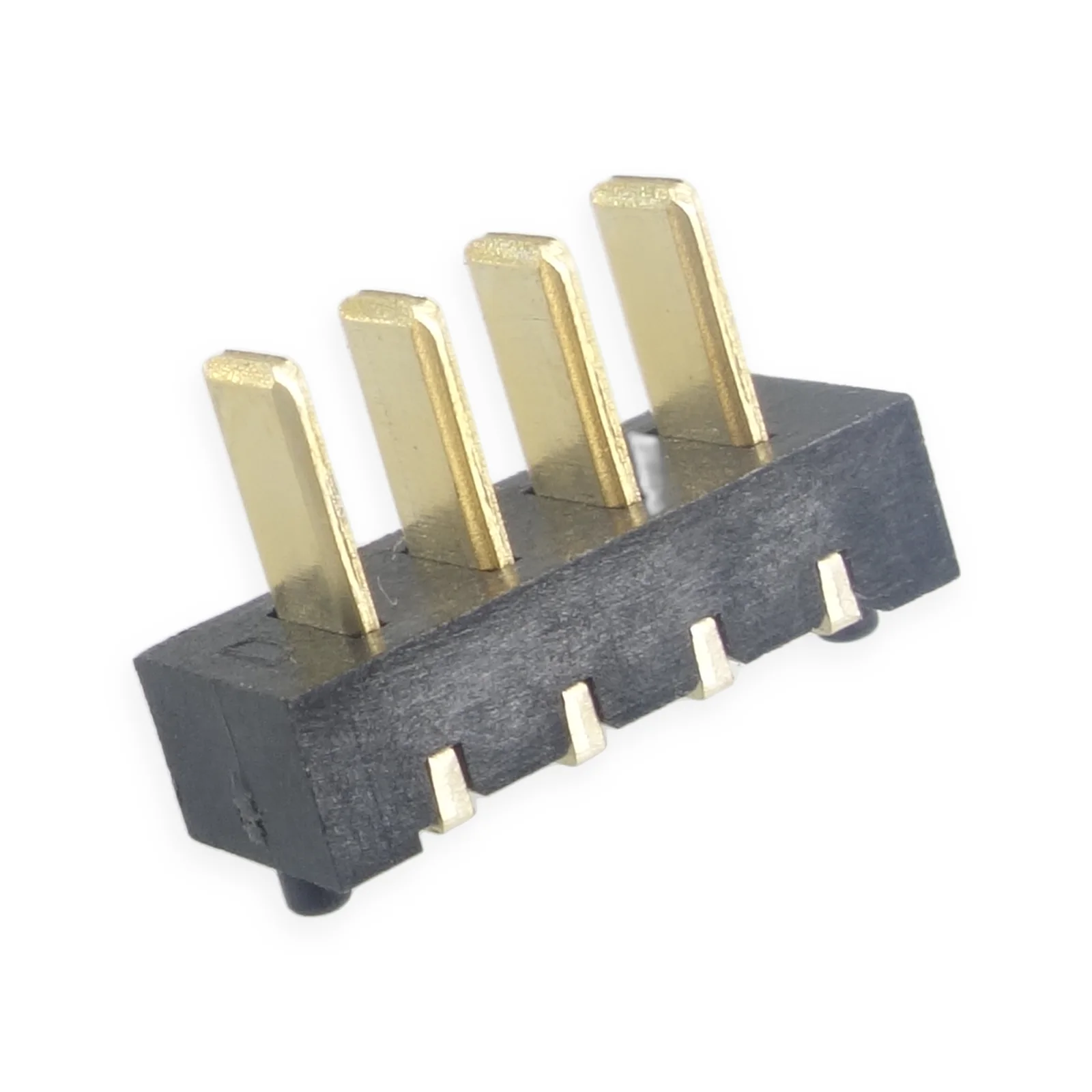
Start with the exact solder-tail style, its PCB layout and the support around the connector: an SMT blade header needs seated solder feet and correctly placed pads, while a right-angle through-hole receptacle needs the matching holes, tail clearance and board support.
For a removable battery interface, these details belong in the design review before the PCB is ordered. The mating face may look simple, yet its forces reach the housing, locating features, board and solder joints together. This guide uses the four-position drawing row for Kangsheng KS-2.5-M-VSMTPOST and the B04F-4P-L2 drawing attached to KS-BL-352 to show what to check on each board side.
Key takeaways
- Select the exact contact count and tail version before creating the footprint.
- Record contact-face, board-side and side views against one pin reference.
- Give insertion and withdrawal loads a defined path through the supported assembly.
- Agree the soldering process for the selected part, board and solder materials.
Identify the mounting style from the board side
SMT describes a termination that sits on surface pads. Through-hole describes tails entering holes in the board. Right-angle describes orientation. Keep those descriptions in separate fields: a contact can face a board edge while using a particular board termination underneath it.
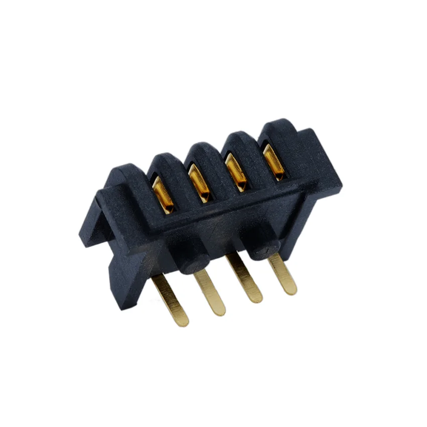
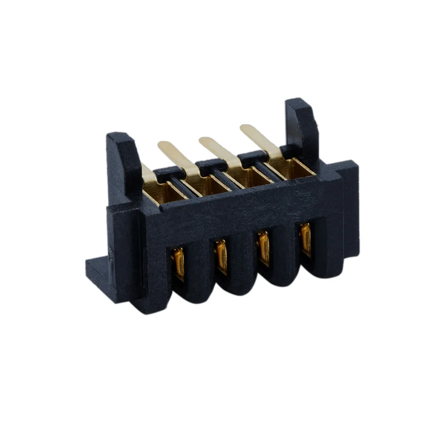
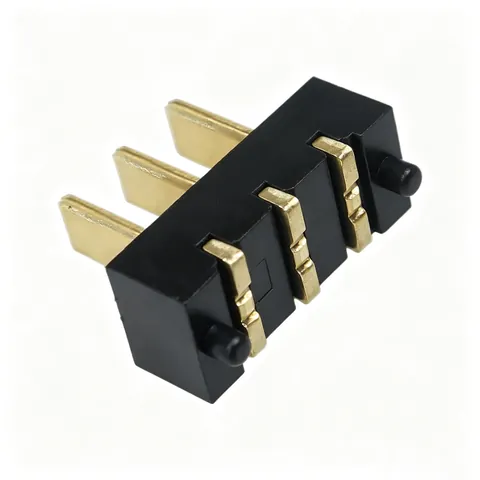
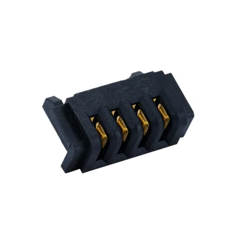
The KS-2.5-M-VSMTPOST example has upright blades, surface-mount solder feet and locating posts. The selected KS-BL-352 example has a receptacle face and bent through-hole tails. Photograph the contact face and board side separately when identifying samples. Once the tail style is selected, assign it its own footprint and assembly instructions.
Follow the mating force back to the board
When a battery or removable module enters a connector, the assembly must react the insertion force. When it leaves, the direction reverses. Sideways handling can also bend an unsupported board or rotate the connector about its attachment points.
Draw the enclosure guides, mechanical stop, connector housing and nearby board supports in one section. Check which feature aligns the parts first and which feature stops movement at the final position. Locating posts align the connector. Enclosure guides and mechanical stops should react insertion and withdrawal loads so those loads are not carried by the solder tails. Place board support so the intended mating action can be evaluated without unnecessary board movement.
Warning signs during the first assembly
Use these observations to decide where to inspect. Record what happens before assigning a cause.
| Observation | Area to inspect | Useful check |
|---|---|---|
| Housing rocks before soldering | Seating and locating features | Compare post positions, holes and the seating plane in the same view. |
| One SMT foot stands above its pad | Part seating, tail condition and PCB surface | Inspect the unsoldered assembly from the side and record the gap. |
| Board moves when the module is inserted | Guides, stops and board support | Observe the assembled load path with the intended mating part. |
| Contact positions align but tails miss the layout | Tail variant and drawing view | Recheck the exact drawing row and pin reference before revising the footprint. |
Why mounting problems appear after a footprint looks correct
A footprint can have the correct nominal pitch while its locating features come from another variant. A contact-face view can also be copied into the board view with the wrong handedness. Both problems become clearer when the drawing views share a marked pin reference and coordinate origin.
Seating deserves a separate check. A locating feature that meets an obstruction can lift the housing and leave the solder feet unevenly seated. During assembly planning, inspect the full body outline, nearby components and access beneath the tails. Include the enclosure and board supports in this review; the bare PCB layout shows only part of the mechanical arrangement.
Where these checks matter in removable devices
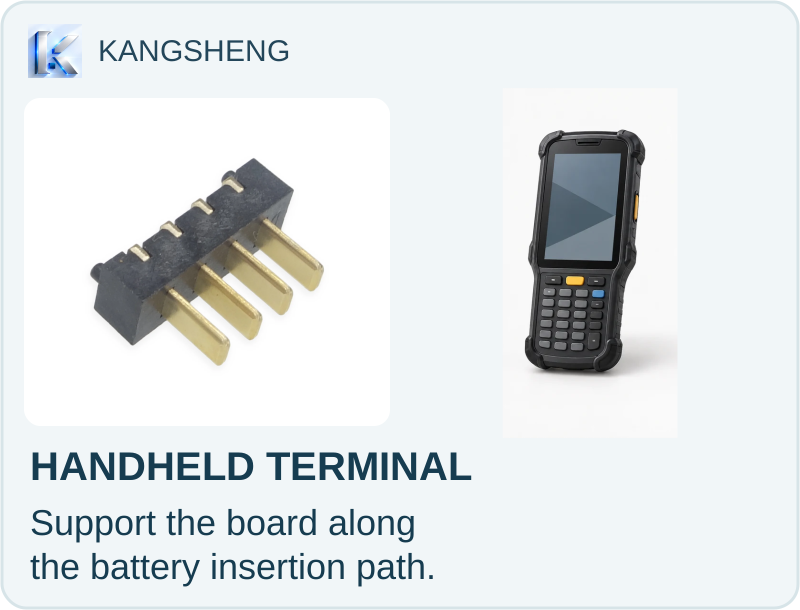
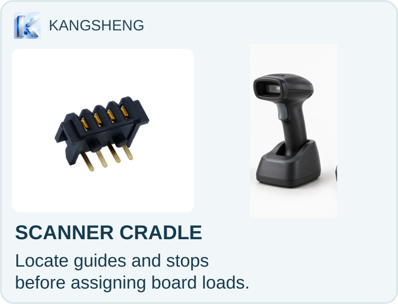
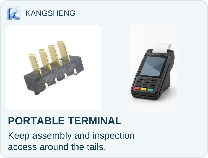
Application illustration: the following cards combine unchanged Kangsheng product photographs with generic AI-generated device images. Each card identifies a mounting question to carry into an assembly review.
Read the four-position dimensions from each drawing
The following values are standard-product drawing values. Select the four-position row in the B01M-R1 family drawing and the specific B04F-4P-L2 drawing for the receptacle.
| Drawing feature | KS-2.5-M-VSMTPOST, 04 row | KS-BL-352, B04F-4P-L2 |
|---|---|---|
| Selected contact count | 4 | 4 |
| Adjacent contact-center pitch | 2.50 mm | 2.50 mm |
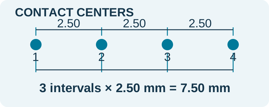
| First-to-last contact-center span | DIM.C: 7.50 mm | 7.50 mm |
| Outline and locating dimensions | DIM.A housing width: 12.00 mm; DIM.B locating-post / PCB-hole center distance: 10.50 mm | Body width: 11.50 mm; wider outline: 14.45 mm |
| Board-side reference | Recommended PCB layout notes T = 1.2 mm | Separate recommended PCB layout for the bent-tail version |
| Electrical drawing values | 5 A / 30 V AC | 7 A; instantaneous 10 A |
For four equally spaced contacts, there are three intervals. The nominal center span is therefore (4 − 1) × 2.50 = 7.50 mm. Use that calculation to check the contact row, then read the pad and hole dimensions from their own layout view. For more on the measurement reference, see the pitch and center-span guide.
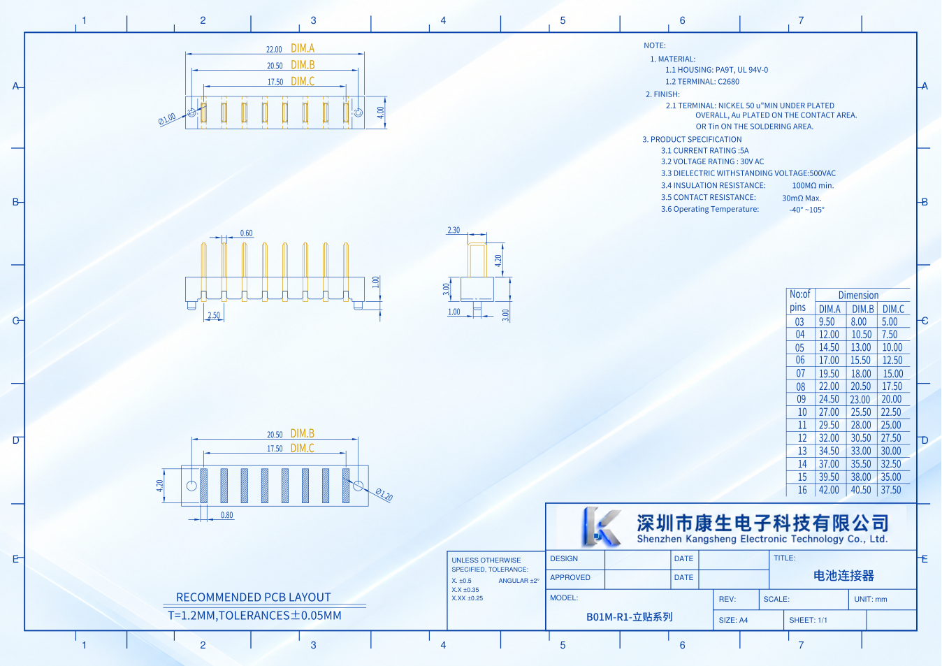
Download the B01M-R1 drawing and identify the selected row in the assembly file.
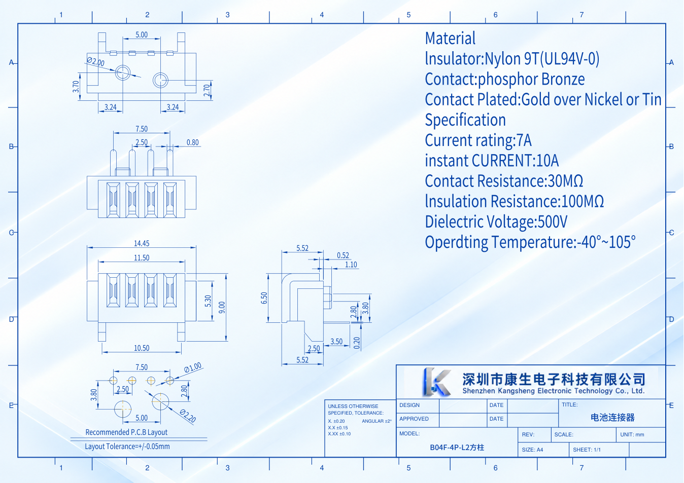
Download the B04F-4P-L2 drawing and retain that filename with the footprint record.
Prepare the soldering process with the assembler
For the SMT version, review pad geometry, solder-mask openings, stencil apertures, placement support and access for inspection. Check that the locating features allow the housing and solder feet to reach their intended seating positions. Agree how the assembly will remain aligned during the soldering cycle.
For the through-hole version, review tail dimensions, finished holes, lands, board thickness and access on the solder side. Include nearby components when choosing the assembly sequence and any required fixture. Ask the assembler to document the soldering method and inspection plan for this board.
Obtain the soldering limits for the exact connector version and combine them with the requirements of the selected solder materials and PCB. Keep the resulting process record with the drawing revision and board build. A soldering recipe should identify the materials and assembly it was qualified for, so later changes can be reviewed against the same record.
Prevent problems before ordering the board
Review the footprint at actual dimensions with the layout designer and assembler. Mark the connector outline, mating direction, board edge, locating features and inspection clearances. Show the nearby supports and the mechanical stop on the assembly drawing.
Check the contact numbering from the mating face through to the board connections. Complete the mating-orientation checks for the specified counterpart, then review the two board-side footprints individually. Keep the selected contact count, tail version and drawing filename visible in the bill of materials and manufacturing package.
If the sample is already tilted or loose
Preserve the sample condition long enough to photograph the joints, seating and surrounding board. Compare it with an unsoldered sample and the selected drawing. Identify whether the next check concerns the connector, footprint, assembly process or mechanical support.
Agree the correction with the responsible designer or assembler, then evaluate a fresh assembly against the same checklist. Record the part and board revisions, what changed, and the observations after the correction. This creates a usable comparison when the project moves from samples to a pilot build.
Make two footprint records before board release
For B01M, select row 04 before transferring the layout. Its DIM.A, DIM.B and DIM.C values are 12.00, 10.50 and 7.50 mm. Trace the B and C arrow endpoints between the dimension table and the board view. The family layout picture shows eight pads; set the selected contact count and row dimensions in the footprint record before arranging the four-position pattern. Carry the T = 1.2 mm layout note alongside the project's actual PCB thickness.
For B04F, use the specific four-position file. Record the four smaller circles and the two larger hole features separately, then trace them to the side view and board-side photograph. Preserve the tail direction, board edge and agreed pin reference when moving between views.
On a narrow screen, swipe the table to compare both drawings.
| Record to keep | B01M, selected 04 row | B04F, selected four-position drawing |
|---|---|---|
| Board termination | SMT pads and locating features | Finished holes and tail clearance |
| Drawing reference | Selected B/C dimensions and PCB view | Hole-layout view and side view |
| Installation check | Seating, nearby support and mechanical stop | Seating, nearby support and mechanical stop |
Keep each record with its own part number, drawing and PCB revision. Review the complete interface against the project's approved mating drawing.
Kangsheng can customise solder-tail form and connector height to suit the customer's PCB layout.
What to send Kangsheng
Kangsheng Electronics (Shenzhen Kangsheng Electronic Technology Co., Ltd.) provides the product photographs and PDF drawings linked here. Use the KS-2.5-M-VSMTPOST page or KS-BL-352 page to identify the candidate.
Explore the 2.5 mm blade connector series when comparing other board-side variants.
Send the exact part and contact count, required tail style, PCB thickness, footprint view, available assembly space and mating-side drawing. State whether the current request is for drawings, samples or a quotation, and list the mounting questions that need an answer.
Send the mounting question with your drawing
Use the enquiry form to share the exact candidate, PCB view and mating-side drawing. Identify the tail style, contact count and requested sample quantity, then list the questions about seating, support or soldering that the next review should resolve.
CATALOGUE REFERENCES
Related products
Frequently asked questions
Does 2.5 mm pitch define the PCB footprint?
Is a right-angle connector always through-hole?
Do locating posts settle the board-support question?
Can one soldering profile cover both examples?
What should the first sample review record?
YOUR NEXT DESIGN CHECK
Review your PCB footprint.
Send the selected part drawing, pin reference and PCB constraints for a mounting review.
Ask about this article